Why Make This?
A couple of months back I decided to try making an analog function generator. My requirements were pretty loose, I just wanted to see if I could generate some square, triangle, and sine waves. Additionally, I wanted to be able to adjust the frequency and amplitude of the waves generated. This actually turned out to be pretty easy, only taking three op-amps.
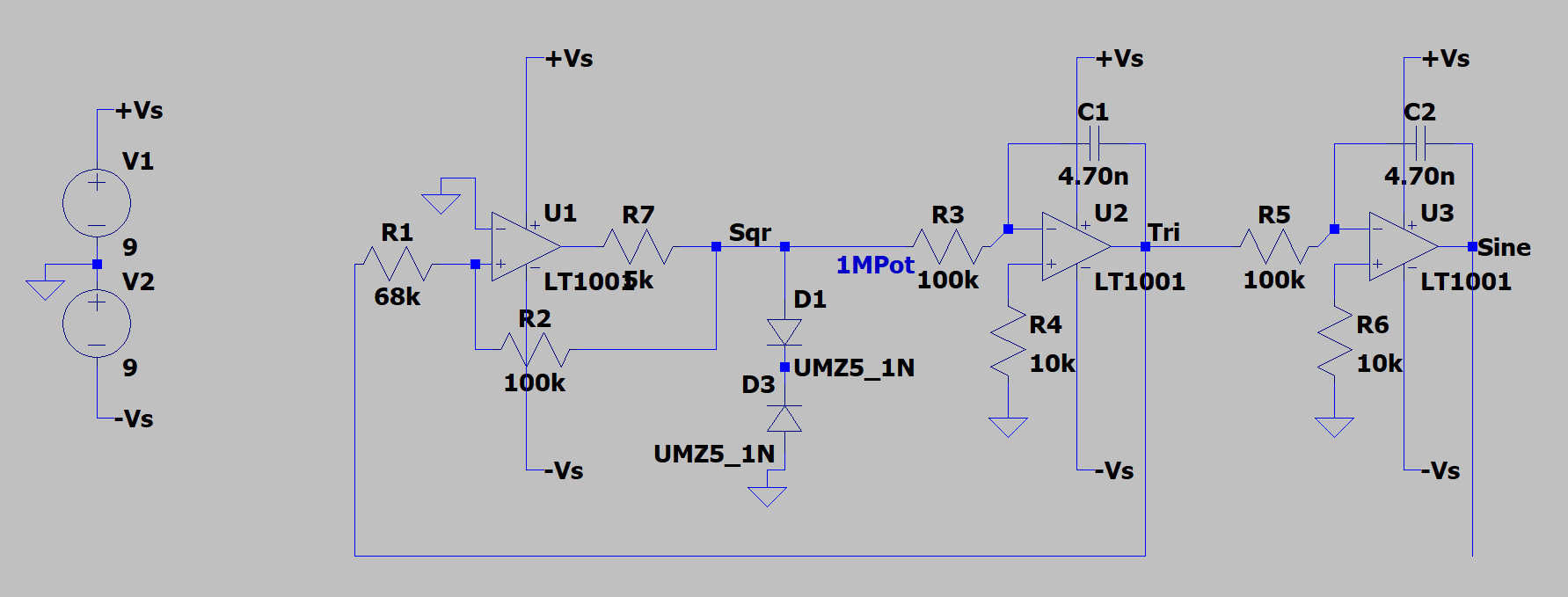
The problem with this circuit is that it’s extremely limited in its bandwidth. This is because of the capacitors used in the integrators for the sine and square waves. As the frequency of the waveform rises, the capacitor presents less and less impedance so the waveform travels ‘around’ the op-amp via the capacitor. This causes the amplitude to drop, as the op-amp is what’s responsible for amplifying the waveform. Thus, our output waveform drops as our frequency rises. Pretty undesirable for a waveform generator.
What is an AGC? Why a Gilbert cell?
So our problem is that as the frequency rises, the op-amps become increasingly shorted. One way to stop this would be to swap the capacitors so that they present a higher impedance at higher frequencies. Or we could even swap out the amplifier topology entirely to circumvent this issue.
Another way would be to simply generate the signal, and then amplify the signal back to a desirable level afterwards. This method doesn’t involve modifying our current waveform generation circuit but instead adds another stage entirely. This stage would be responsible for amplifying the generated waveform so that it maintains a constant amplitude, in our case 5 volts peak-to-peak.

Very professional diagram of an AGC loop.
So for this secondary stage we have an input signal (the output of the function generator), which will have a varying amplitude. To maintain a constant amplitude we must apply a dynamic gain in order to respond to the variations in input amplitude. This process is known as automatic gain control (AGC). In this post we’ll begin by implementing a voltage controlled amplifier (VCA), which is an amplifier whose gain varies with a control voltage. In order to go from a VCA to AGC, we’ll need to implement a feedback loop to dynamically adjust this control voltage such that a constant output amplitude is maintained, although I won’t be discussing that in this post.
This is not a typical application for an AGC. To be honest, simply changing the function generator topology would be a better way to achieve a function generator with a desired output range and bandwidth. While the function generator is what got me started designing this AGC, at this point I am much more interested in designing a stand alone AGC whose capabilities would make it adequate for improving the bandwidth of the three op-amp function generator as well.
The rest of this post will discuss the design of the VCA; for which I’ve decided to use a Gilbert cell. It’s capable of multiplying voltages which means it’s capable of dynamic voltage controlled gain, and it’s also frequently used in RF applications which means it should be able to handle our desired frequency range of 1hz-1Mhz. Let’s first get an overview of how a gilbert cell works.

Full Design. We’ll be going through it piece by piece in this post.

Multiplication of two sine waves.
How does a gilbert cell work?
A gilbert cell is composed of 3 differential pairs. To keep everyone on the same page, I’ll quickly cover how a differential pair works. For those who already know, feel free to skip the next three paragraphs.
A differential pair is a differential amplifier which consists of two input transistors ending in a shared tail. Unlike single ended amplifiers, differential amplifiers take in two inputs and amplify the difference between them. The differential pair’s ‘tail’ is typically biased with a constant current and inputs are supplied at the base of either transistor. This difference in the input voltages causes the transistors to carry different amounts of current, however the sum of the current in either branch will always equal the bias current.

So in essence a differential pair takes in a voltage differential and outputs a current differential proportional to the input. By attaching load resistors at the output we are able to convert this differential current back into a differential voltage signal at the output node. The differential gain of this circuit can described by
$A_v = -g_m \cdot R_L$
Where $R_C$ is the load resistance placed at the collector. The transconductance ($g_m$) of a transistor is found by $I_c/V_t$ where $I_c$ is the current through the collector of the transistor and $V_t$ is the thermal voltage, approximated at 25mV. These equations mean that we can vary the gain of our differential pair by varying the current through the transistors! If we increase the bias current the gm increases with it and as a result the gain does as well. Similarly, if we decrease the bias current, we can reduce the gain. This allows us to change the gain. While a simple differential pair would be a viable candidate to create a VCA, there is an alternative topology which boasts a better frequency response.

The gilbert cell is typically found as a mixer in radio frequency applications. It consists of three differential pairs, two on the top layer and one on the bottom.
Let’s start by looking at the top two differential pairs. There’s only two things you really need to notice to understand how these work.
- The two pairs are wired inversely of each other. This means that for any given input differential, $V_{in}$, one pair will receive $+V_{in}$ and the other will receive $-V_{in}$.
- Their outputs are joined together such that their currents sum at the output.

Because the differential pairs receive inputs equal in magnitude but opposite in direction, their output current will also be equal in magnitude and opposite in direction. That means if both pairs are biased with an equal tail current, the output current will always be zero.
This is where the bottom differential pair comes in: By placing the top differential pairs as the ’load’ of each leg of the bottom differential pair, we are able to steer the current from one of the top differential pairs to the other, making the gain either more positive or negative depending on which load differential pair we drive more current through. Notably, the output of the gilbert cell will always be zero if either of its inputs are zero and the output itself is proportional to the product of the two input voltages. This is, loosely speaking, a multiplication of two voltages!

Joined vs split tail differential pair.
You may notice that sometimes the bottom ’tail’ of the differential pairs are split or joined throughout this post. They’re functionally equivalent to each other, although they respond differently to mismatch between components. The split style responds better to differential pair transistor mismatch which is why I’ve opted for it in the design.
Biasing the Gilbert Cell

The goal when biasing a gilbert cell is to ensure that all transistors stay in the active region for the desired input and output ranges while maximizing the voltage headroom for the output signal. We’ll be using a resistor tree in order set the dc operating point for our differential pairs. In our case we have to account for the voltage drop of four things:
- The current sink
- The bottom differential pair
- The top two differential pairs
- The load resistors
The transistors require, at minimum, a voltage of 0.2 volts between the collector and emitter to stay in their active region so we’ll need to ensure $V_{CE}$ > 0.2 volts throughout the input and output range. Otherwise, the transistor will saturate and we’ll risk cutting off or otherwise distorting the output waveform.
Let’s start by looking at the bottom differential pair. We know that $V_{CE}$ must be greater than 0.2 volts at all times during normal operation. We also know that our input will be fed to the base of the transistor and that $V_{BE}$ will always be around 0.6-0.7 volts. So, as the base voltage moves in unison with our input, we know $V_{E}$ will move with it as well, merely level shifted by -0.6 volts.

$V_B$ and $V_E$ move in unison.
Since our input and emitter voltage move in unison, we must bias our bottom differential pair with exactly how much voltage we desire for our input range. In our case, I chose ±2 volts. This means we’ll need to bias our bottom differential pair so that it has 2 volts in either direction, so we’ll have 4 volts of voltage headroom dedicated towards the bottom differential pair. Throwing in the voltage drop required by the current mirror below the bottom differential pair, we end with a headroom cost of 5 volts. we can bias our bottom differential pair at 5 volts above our negative supply, which in our case is -4 volts.
Let’s look at biasing the top two differential pairs now. Just like the bottom differential pair, $V_{BE}$ will remain at 0.6-0.7 volts throughout normal operation. However, due to the extra input differential pair (explained later), the input to the top differential pair only varies by <0.1 volts and so $V_{E}$ does not move appreciably. It is therefore negligible for biasing purposes. This is also why we did not have to concern ourselves with the movement of $V_{C}$ for our bottom differential pair as the two are shorted.

While our top differential pairs’ emitter voltage does not move appreciably, their collectors are tied directly to both $V_{out}$ and our load resistors. This means, similar to in the bottom differential pair, their collecter voltage moves in unision with their respective output node. This relation is described by $-I_{1,2}R_L$ where $I_{1,2}$ represents the current for each of the top two branches. We must bias the top level differential pairs so that even when an output node is at its minimum allowable value the transistors still maintain a $V_{CE}$ > 0.2 volts. In our case the maximum desired output swing is 11 volts. Adding 0.3 volts to ensure a $V_{CE}$ greater than 0.2v leaves us with a bias value of 11.3 volts below $V_{CC}$. Because our circuit runs on a ±9V supply this means the top differential pairs are biased at -2.3 volts.
How do we ensure that at our max input range the load resistor will be dropping 11 volts? Knowing that $V_{out} = V_{CC}-IRL$ and that $I_{max} \cdot R_L = 11$ we know that $R_L = 11/I_{max}$ will ensure we drop 11 volts when our inputs are each at max. In our case, each leg of the bottom differential pairs is biased with 1ma and therefore $I_{max} = 2mA$. So, $R_L$ = 5.5k.
With this, we’ve ensured that the bottom and top differential pairs will avoid collector-emitter saturation for our desired input and output range. While biasing the operating points allows us to avoid $V_{CE}$ saturation, it doesn’t prevent saturation due to current steering. For that, we turn our attention to a different technique.
Emitter Degeneration

While we no longer have to worry about collector-emitter saturation, we have yet to deal with saturation due to current steering. This occurs when all current flows through one branch. Let’s look at our bottom differential pair, which we’ve biased for an input range of ±2 volts. But what if it only took ±1 volt to get all current flowing through a branch? Then raising the input past 1 volt would no longer meaningfully affect the output and our waveform would appear “clipped” at the peaks or otherwise distorted.
To find the voltage level at which current steering saturation occurs, we calculate the voltage differential required to drive all current to one branch. This voltage represents the maximum meaningful input differential, and is a function of the bias current flowing through each transistor’s emitter and the effective resistance of the transistors.

$r_e$ models the internal resistance of the transistors emmiter
$\Delta V_{in} = 2I_{e} \cdot r_{e}$
Where $I_e$ is the bias current flowing through each emitter and $r_{e}$ is the effective resistance of the emitter. $r_{e}$ is found by dividing the thermal voltage by emitter current, $V_t/I_e$. Approximating $V_t$ as 25 mV and knowing our emitter current bias is 1mA, $r_{e}$ = 25 Ohms. Without emitter degeneration it only takes 50mV to steer all current to one transistor! As you can imagine, such a limited input range would be impractical for our circuit.

Joined and split tail emitter degenerated differential pairs. They’re functionally equivalent.
This can be remedied by placing a resistor, $R_{e}$, in the tail of the differential pair. This is known as emitter degeneration. In doing so, the resistor is directly added to the effective resistance of the emitter yielding:
$\Delta V_{in} = 2I_e \cdot (r_e + R_{e}) \approx 2 I_e R_{e} \quad \text{when } R_{e} \gg r_{e}$
This allows us to change the input voltage required to steer all current to one branch. Naturally, this reduces the gain of the circuit as more voltage is required to steer the same amount of current, however it also results in increased linearity. This is because at the edges of our input range the gain actually reduces slightly, and by spreading this change out over a wider input range we “smooth out” the change in transconductance ($g_m$)
In our circuit, we desire a 2 volt differential required to swing all current to one branch. Knowing our bias current is 1mA for each transistor and using the equation above we can determine that this requires a 2k emitter resistor.
Why a separate differential pair input?

If emitter degeneration allows us to expand our input voltage range, why haven’t we used it for our top differential pairs? If you remember from when we determined the bias points for our transistors we found that because the base of the bottom pair’s transistors were being directly driven by the control voltage, the input range for the bottom pair had a one-to-one cost on the voltage headroom. While this was a feasible cost when it was just 4 volts, what about 11? Such a cost on headroom would only leave us with ±1 volts for our output signal. Pretty undesirable.

In order to allow us a large input range we’ll need to somehow avoid the one-to-one relationship between input voltage and the emitter voltage of the top transistors in our gilbert cell. To do this we’ll first put the input voltage through a differential pair in parallel with the gilbert cell, in effect “side-loading” the input range, decoupling our input signal from the emitter voltage of the top differential pairs. This side-loaded differential pair once again has access to 18 volts of voltage headroom, and can easily accommodate an input range of ±5.5 volts by way of a 5.5k emitter resistor.
How should we load the output of our input differential pair? One option would be resistors, however these would need to attenuate our signal to ± 50mV. This would demand precise resistor values and would also be sensitive to mismatch. If we overshoot ±50mV our gilbert cell will saturate and distort or clip at the output. If we undershoot ±50mV we diminish our gilbert cell’s output range. Another more appealing option is diode connected transistors.

Diode connected transistors are transistors which have had the collector and base shorted and therefore act like diodes (as the name might suggest.) The reason that a diode load is desirable is because its current depends exponentially on its forward voltage. Because of this, we can express a large change in current with a negligible change in voltage. In our case, we are able to express our desired maximum current swing in ~50mV.
Here’s another way to look at it: A differential pair converts a voltage ratio to a current ratio, and by doing so it converts our voltage signal to a current signal. When we use a resistive load, we are in effect converting that current signal back to a voltage signal at the output node. However by using a diode connected load we maintain the signal as a current. Because transistors are effectively current controlled current sources we are still able to achieve adequate amplification despite a small input voltage swing as long as the current swing is large enough. One other notable benefit of a diode connected load is that by maintaining a relatively constant voltage across the input signal range, the early effect is greatly reduced and there is a reduction in non-linearity.
In conclusion, by conditioning our top input voltage before passing it to the top two differential pairs, we are able to expand the input voltage range while avoiding a costly reduction in the output range of the gilbert cell. One final note is that this input differential pair is capacitively coupled to the top two differential pairs of the gilbert cell. This method of coupling has a few drawbacks to it which will be discussed later. Ideally, it would be best to directly couple these two stages.
Current Biasing

For our current source, I opted for a slight modification of a basic current mirror. A basic current mirror topology consists of a NPN transistor with its collector and base shorted. This creates a ‘self-biasing’ transistor, which sets its own base voltage and current. This voltage and current are dependent on how much current flows through its collector. Then, by connecting this node to other transistors’ bases we can ensure that they also pass that much current through their collector, in essence ‘copying’ the current from our reference branch.

You might notice there is a transistor wired in between the collector and base of the transistor in our reference branch. That’s because I’ve implemented a current mirror technique known as base-current compensation. The new transistor is responsible for supplying the base current to the mirror transistors. In doing so, it reduces the error between the copied current branches and the reference branch by a factor of its beta.

The resistors placed below each current sink transistor are responsible for emitter degeneration. Their purpose is twofold.
- They stabilize the output current by increasing the output resistance of each current sink and providing negative feedback at the emitter node.
- They also allow us to modulate the amount of current sunk by each branch by changing their value. Our circuit is designed so that at 1k ohms the transistor sinks 1mA, however if we dropped the emitter resistor of any branch to 500 ohms instead the transistor would then sink 2 mA.
As for bias current, I’ve opted for 1mA. This was done to minimize the power dissipation of the circuit and our circuit still provides a moderate gain. The transistors used have the highest hfe when biased with 10mA, however this would come with 10 times increased power cost. I believe that in the future increased open-loop gain will be a necessity and the bias current is one area to look at.
Frequency analysis

I ran a frequency analysis in LTSpice. The results were better than I expected for a first pass at the circuit! The -3dB point lies at ~5MHz which far surpasses the desired bandwidth. The unity gain point occurs at ~44MHz. You might notice the ‘ramp up’ at the lower frequencies only reaching our peak gain at ~20kHz. This is because the input differential pair is capacitively coupled to the gilbert cell and is one reason motivating a future move to direct coupling. However for a general purpose broadband AGC, I believe this frequency response is acceptable.
SFDR Analysis

Yikes! Tested with a 2 volt control voltage and 11 volt pk2pk sine wave
SFDR (Spurious Free Dynamic Range) is a metric which lets you see how ‘pure’ a waveform is. It’s the difference in amplitude, in decibels, between the desired output frequency and the largest undesired output frequency (known as a spur). In our case the SFDR with a max input range sine wave is ~30dB. This is pretty bad! For adequate audio, the minimum SFDR is somewhere around 50-60 dB and anything below this will sound audibly distorted.
I believe the cause for distortion is the nonlinearity which comes with using the full range of a differential pair. One potential modificiation would be lowering the input range and increasing gain so that we can stay closer to the quiescent current of the differential pair, where the gain is more linear. For now I ran another fourier transform with a smaller input wave, only 5 volts pk2pk. The SFDR increased to ~50dB, which isn’t amazing but definetly better.

Tested with a 2 volt control voltage and 5 volt pk2pk sine wave
Conclusion and Next Steps
The Good:
- It works!
- I’m pretty pleased this thing works at all, even if it’s going to need quite a bit of tweaking before being ready for integration into an AGC feedback loop.
- The upper cutoff frequency is quite good
- The upper bandwidth far exceed my expectations, easily clearing the 1Mhz desired.
The Bad:
- The lower cutoff frequency is quite bad
- Due to the capacitive coupling between the input differential pair and the Gilbert cell, the lower cutoff frequency is much higher than the targeted 1Hz. A move to direct coupling in future revisions of this circuit will likely resolve this issue.
- Very low SFDR
- The circuit is currently distorting input signals quite a bit. I have a suspicion this is due to the variance in $g_m$ across a differential pairs input range. Using less of the input range seems to alleviate this somewhat, however this alone is not satisfactory.
- It’s possible the variations in voltage across the current sinks or the diode connected loads in the input differential pair are contributing to distortion as well.
- The gain is low
- For a negative feedback loop, the higher the open-loop gain better. With a maximum control voltage, this gilbert cell has a gain of less than 2!
- This is mostly due to emitter degeneration. At the beginning of this project, I wasn’t familiar with how negative feedback loops worked.
- I’m likely to raise the gain in the future by raising the current drawn by the current sinks, trading off with power dissipation. I’ll also likely reduce or remove the emitter degeneration for the bottom pair entirely.
Overall, I believe these results are quite promising for a first iteration of the circuit. I’m particularly pleased with the bandwidth of the circuit, and it would be nice to see even half the simulated bandwidth once built.
The next steps for this project involve designing the other components necessary for the feedback loop of the AGC, as well as addressing the shortcomings of the current revision of the Gilbert cell. For the AGC loop, we’ll need a means of sensing the output wave forms amplitude, and a means of modifying the control voltage in response to the change in output amplitude. While a simple peak detector can detect the output amplitude of a waveform, it does so at a limited frequency range, so a design with a wider frequency range will be needed. We’ll also need a way to compare this peak with a reference voltage (our desired amplitude). While an op-amp could work here, I’m also interested in seeing if any transistor based solutions fit the bill.
I’d also like to begin prototyping the Gilbert Cell. I’ve ordered some matched transistor pairs, and look forward to building it soon. I’ll probably start with some jumper wires for a first pass but I’d also like to design a PCB for this project.
If you’ve made it this far, thanks for reading! I really appreciate it. I love to talk about this kind of stuff so if you have any questions or feedback feel free to shoot me an email!