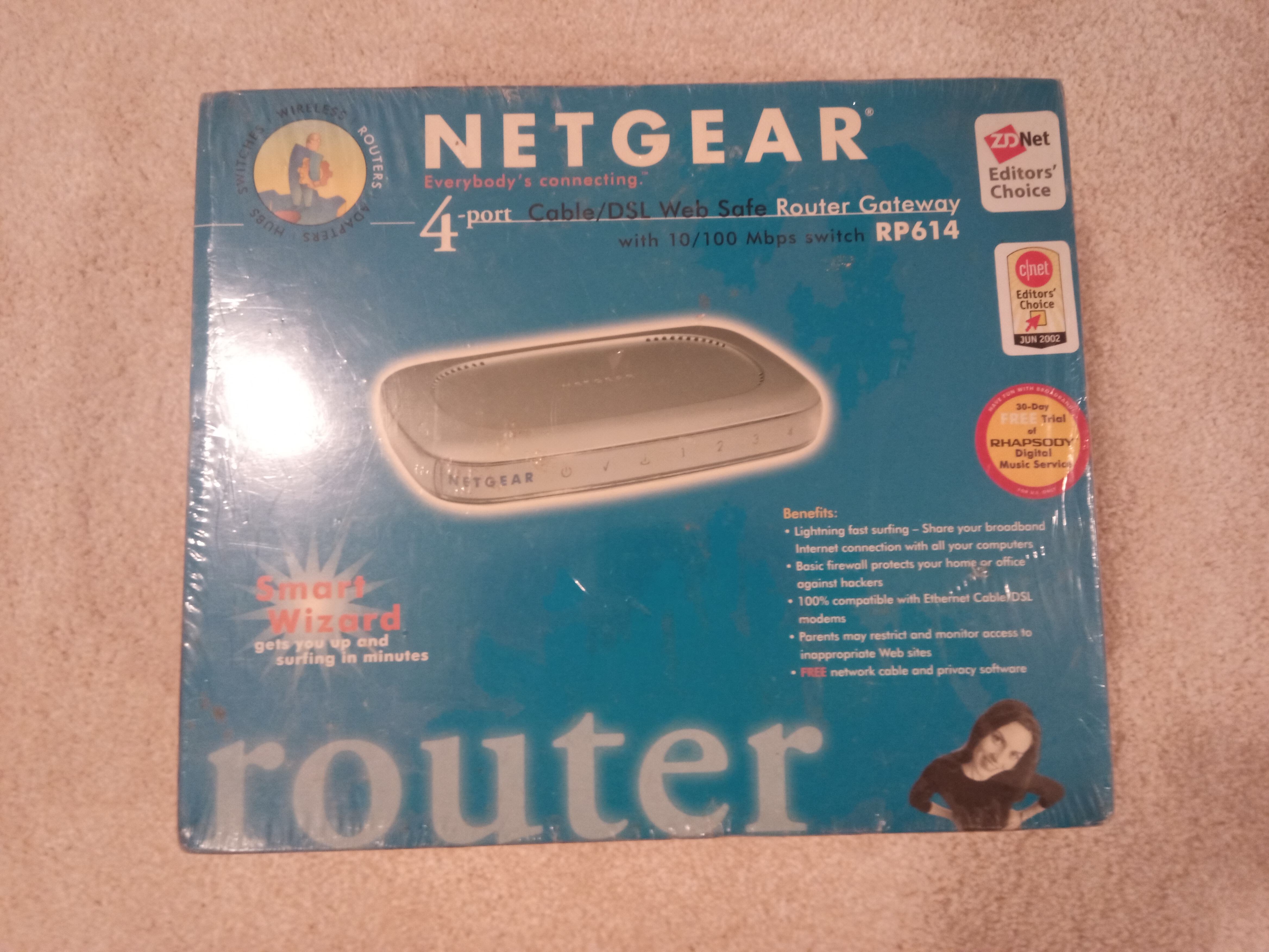
A couple months back I was introduced to the concept of hardware hacking. It seemed like a really interesting area to dive into, so at Anna’s suggestion I decided to start by attempting to reverse engineer an old router, with the goal of getting the program memory off of the device, and eventually reverse engineering the firmware itself. After searching online, I found an old Netgear RP614 for sale. Still in the plastic wrap too!
The first thing I did with the router was take it apart. Looking inside, we can begin to guess how this thing might work.
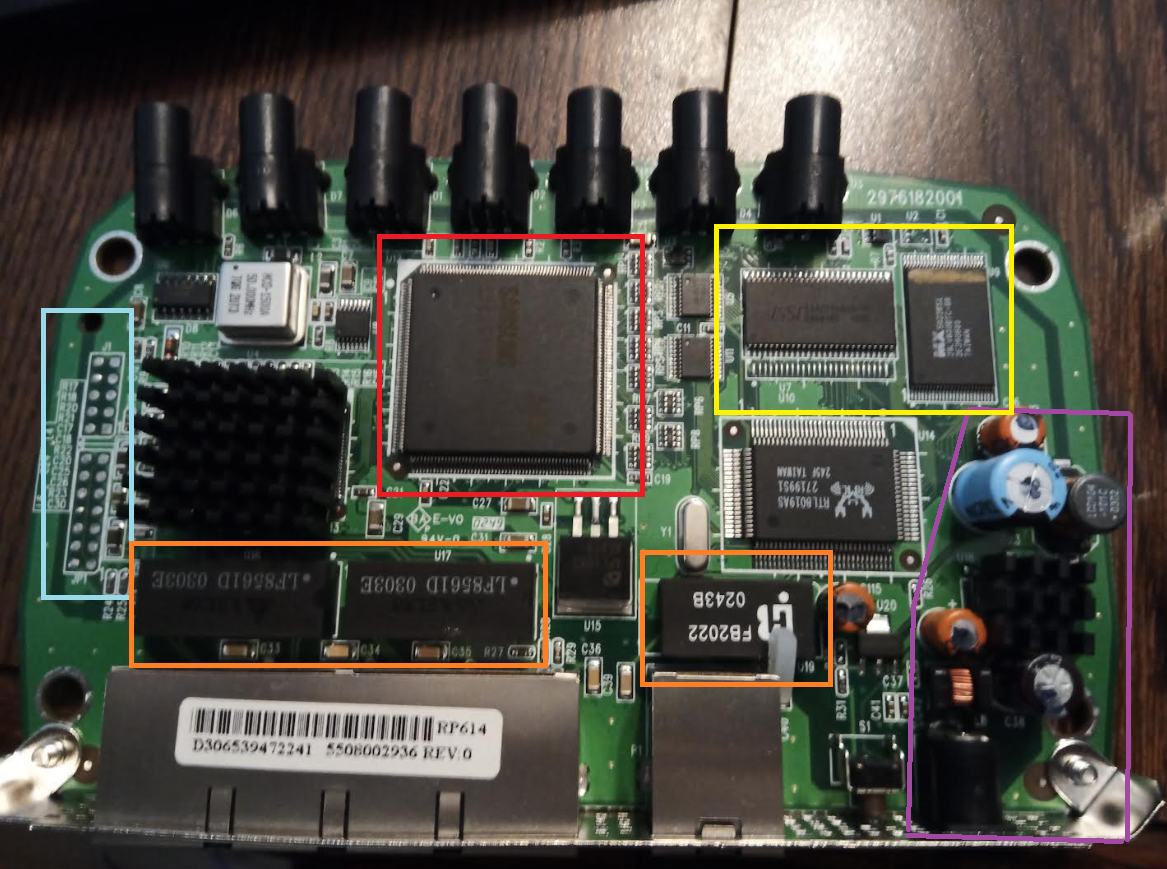
By inspection, we can begin to divide the board into sections. The first area is the power circuitry around where the 12V dc line comes in. This is unlikely to be of much interest to us. Next, we have the biggest chip on the board, and what appear to be memory chips. The big chip is likely our CPU with the two rectangles off to the side being likely candidates for ROM/RAM chips. We also have ICs right near our ethernet ports, as well as that crab one and our mystery chip under the heatsink.
To my surprise, I was able to find datasheets for most of the chips on the board! Our CPU is an S3C4510B01, a Samsung chip specifically for routers. It’s an ARM7TDMI RISC processor, with 2 UART channels and support for external memory and JTAG debugging. Our two suspected memory chips are external RAM and flash chips which are connected to our CPU. The IC before the ethernet ports is a RTL8019AS, a full duplex ethernet controller. To be honest, I didn’t feel like taking the heatsink off our mystery chip (I have no way of replacing it) but I believe it’s safe to assume that it is also an ethernet controller of some variety.
At this point I decided to begin looking into our CPU, with the hopes of leveraging access into the CPU to pull flash from the device. The datasheet is a cool 422 pages, and seems to contain just about everything one could want to know about the S3C4510B. Right here on page 5 we have our pin assignment diagram:
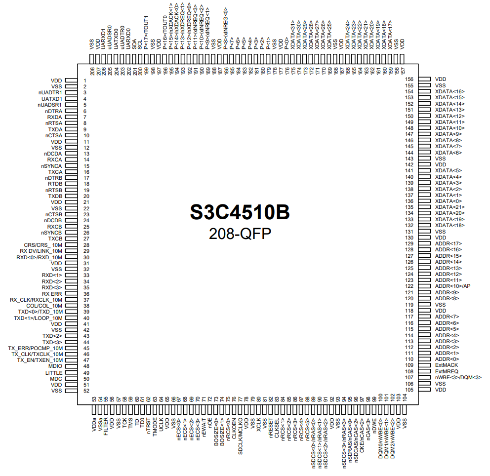
I first tried to connect to the UART interface, in the hopes that I could get access to useful logs or maybe even a root shell if I’m lucky. Using the datasheet as a reference, I hooked into the UART1 pins using my fancy new bus pirate and began monitoring. I booted the device and waited… and saw nothing. I tried probing the second UART interface and got similar results. Welp, guess there’s no UART output!
Afterwards I turned my attention to the JTAG pins. I hooked in again using SMD probes and once again got absolutely nothing. Damn. If there’s no way to gain access to the CPU my only option for accessing the program memory would be by interfacing directly with the flash chip. This would involve either soldering a ton of tiny wires to the flash chips pins or desoldering it from the board. Then I’d have to write a program to interface with the chip and download the memory. Honestly, it sounds pretty fun, but also incredibly tedious and with a lot of room for accidentally damaging the board.
At this point in time I realized I had mistaken which pin on the CPU was pin 1 ༼ ༎ຶ ᆺ ༎ຶ༽
After confirming the orientation of the CPU by counting how far in each VDD pin was by hand (not my idea of fun believe it or not), I retested UART 1 and 2 and got nothing. At this point, instead of placing 5 finicky SMD probes for the millionth time into this chip to test JTAG in the new orientation, I decided to test the pads which were broken out on the side of the board. Something I definitely should’ve done much sooner! I tested which nets the pins shorted to, their resistance to ground and VCC, and their voltage.
10 Pin Connector:
| Pin | RGND (Ω) | RVcc (Ω) | Voltage (V) | Notes | Pin | RGND (Ω) | RVcc (Ω) | Voltage (V) | Notes |
|---|---|---|---|---|---|---|---|---|---|
| 1 | 0 | 3k | 0 | GND | 2 | 0 | 3k | 0 | GND |
| 3 | Inf | Inf | 0 | Visually Unconnected | 4 | Inf | Inf | 0 | Visually Unconnected |
| 5 | Inf | Inf | 0 | Visually Unconnected | 6 | Inf | Inf | 0 | Visually Unconnected |
| 7 | ~60k | ~60k | 0 | Shorts UARXD0 | 8 | ~54k | ~58k | 3.3v | Shorts UATXD0 |
| 9 | Inf | Inf | 0 | Visually Unconnected | 10 | 1.4k | 0 | 3.3v | VDD |
14 Pin Connector:
| Pin | RGND (Ω) | RVcc (Ω) | Voltage (V) | Notes | Pin | RGND (Ω) | RVcc (Ω) | Voltage (V) | Notes |
|---|---|---|---|---|---|---|---|---|---|
| 1 | 0 | ~2.9k | 0V | GND | 2 | ~1.3k | 0 | 3.3V | VDD |
| 3 | Inf | Inf | 0V | 4 | ~60k | ~60k | 0V | Shorts TDO | |
| 5 | 0 | ~2.9k | 0V | GND | 6 | ~60k | ~60k | 0V | Shorts TCK |
| 7 | 0 | ~1.3k | 0V | GND, but why does resistance change? | 8 | ~60k | ~60k | 2.4V | TMS |
| 9 | 0 | ~3k | 0V | GND | 10 | ~60k | ~60k | 2.4V | TDI |
| 11 | 0 | ~3k | 0V | GND | 12 | 12k | 10k | 3.25V | Maybe a reference? Doesn’t short to Samsung |
| 13 | 0 | ~3k | 0V | GND | 14 | ~3k | 0 | 3.3V | VDD |
Our smaller test pad array goes to UART, which tells us they likely used that protocol for debugging during development and disabled it before shipping out production versions. Our larger pad seems to connect to a JTAG test access port and after soldering pins I was able to connect to the chip using a J-Link. We’re in!
The next step is actually pulling the program memory from the board. Pulling memory using J-Link Commander is pretty easy, it’s just a single command: savebin <FileName> <StartAddress> <NumBytes>
The problem is, how do we know how many bytes we need to pull? And how do we know our start address?
Well that first question’s actually pretty easy to answer. Our flash chip stores one megabyte, and our RAM stores 8 so we know how many bytes to expect from our memory. For that second question, we’re gonna have to learn about how the S3C4510B handles external memory addressing.
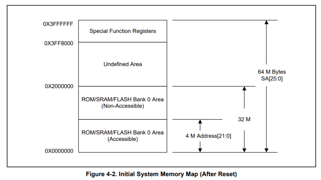
The S3C4510B dynamically allocates memory addresses to external memory chips via special function registers. These get their own bank in memory whose start address is defined by the SYSCFG register.
pg4-5
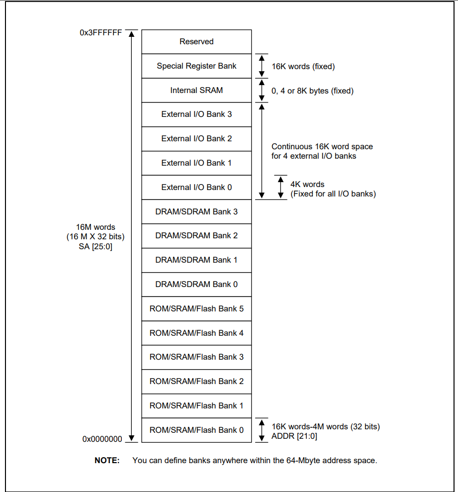
pg4-3
The SYSCFG register is initialized to 0x3FFFF91 by default. Using the chart provided by the datasheet on page 4-20 we know this means the default start address for the special register bank is 0x3FF0000. We can confirm this by connecting via JTAG and stepping through the router line by line.
After booting, one of the very first things the router does is set the value of address 0x03FF4008 to 0x003FFFFF. The offset 4008 corresponds to the INTMSK register, and by setting it to 0x003FFFFF the chip masks all interrupts. This information alone is enough to safely assume that the special function register’s base address is 0x03FF0000 but we can confirm this by reading that address.


Knowing our value is 0xE7FFFF96 and using the information on page 4-6 of the datasheet we can confirm our special function register bank’s base pointer is 0x03FF0000!
After stepping through a bit further we eventually see the CPU execute a store multiple command at offsets 0x3010 - 0x303C, which is how the datasheet requires the MEMCON registers to be set. We care about the ROMCON0 and DRAMCON0 registers which are responsible for setting the base address for the ROM bank, which are found at offsets 0x3014 and 0x302C, respectively.

After decoding these values using the datasheet we get base pointers of 0x0 for ROM bank 0, and 0x1000000 for DRAM bank 0. We now know the memory addresses for ROM and RAM! This is assuming of course that the program utilizes bank 0 for both of its external memories, which is an assumption I’m choosing to make now, and regret later (◕‿◕) 👍
With that, we can simply use the savebin command to grab our ROM and DRAM banks and upload them to Ghidra. We’re now ready to begin reverse engineering the firmware in part two!
I’d like to thank Anna Staats for her guidance throughout this project. All mistakes are solely mine.